


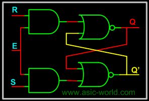
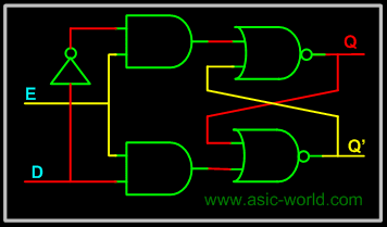
RS Latch with Clock
We have seen this circuit earlier with two possible input configurations: one with level sensitive input and one with edge sensitive input. The circuit below shows the level sensitive RS latch.
Control signal "Enable" E is used to gate the input S and R to the RS Latch. When Enable E is HIGH, both the AND gates act as buffers and thus R and S appears at the RS latch input and it functions like a normal RS latch. When Enable E is LOW, it drives LOW to both inputs of RS latch. As we saw in previous page, when both inputs of a NOR latch are low, values are retained (i.e. the output does not change).
Setup and Hold Time
For synchronous flip-flops, we have special requirements for the inputs with respect to clock signal input. They are
- Setup Time: Minimum time period during which data must be stable before the clock makes a valid transition. For example, for a posedge triggered flip-flop, with a setup time of 2 ns, Input Data (i.e. R and S in the case of RS flip-flop) should be stable for at least 2 ns before clock makes transition from 0 to 1.
- Hold Time: Minimum time period during which data must be stable after the clock has made a valid transition. For example, for a posedge triggered flip-flop, with a hold time of 1 ns. Input Data (i.e. R and S in the case of RS flip-flop) should be stable for at least 1 ns after clock has made transition from 0 to 1.
If data makes transition within this setup window and before the hold window, then the flip-flop output is not predictable, and flip-flop enters what is known as meta stable state. In this state flip-flop output oscillates between 0 and 1. It takes some time for the flip-flop to settle down. The whole process is called metastability. You could refer to tidbits section to know more information on this topic.
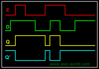
The waveform below shows input S (R is not shown), and CLK and output Q (Q' is not shown) for a SR posedge flip-flop. 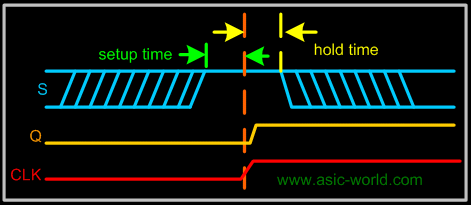
D Latch
The RS latch seen earlier contains ambiguous state; to eliminate this condition we can ensure that S and R are never equal. This is done by connecting S and R together with an inverter. Thus we have D Latch: the same as the RS latch, with the only difference that there is only one input, instead of two (R and S). This input is called D or Data input. D latch is called D transparent latch for the reasons explained earlier. Delay flip-flop or delay latch is another name used. Below is the truth table and circuit of D latch.
In real world designs (ASIC/FPGA Designs) only D latches/Flip-Flops are used.
| D | Q | Q+ |
| 1 | X | 1 |
| 0 | X | 0 |
Below is the D latch waveform, which is similar to the RS latch one, but with R removed.
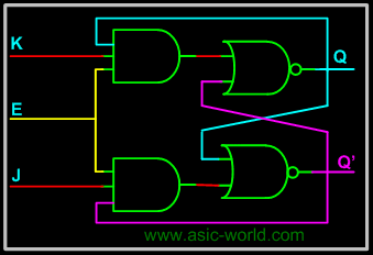
JK Latch
The ambiguous state output in the RS latch was eliminated in the D latch by joining the inputs with an inverter. But the D latch has a single input. JK latch is similar to RS latch in that it has 2 inputs J and K as shown figure below. The ambiguous state has been eliminated here: when both inputs are high, output toggles. The only difference we see here is output feedback to inputs, which is not there in the RS latch.
| J | K | Q |
| 1 | 1 | 0 |
| 1 | 1 | 1 |
| 1 | 0 | 1 |
| 0 | 1 | 0 |
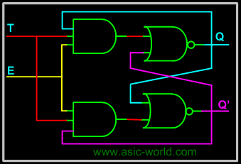
T Latch
When the two inputs of JK latch are shorted, a T Latch is formed. It is called T latch as, when input is held HIGH, output toggles.
| T | Q | Q+ |
| 1 | 0 | 1 |
| 1 | 1 | 0 |
| 0 | 1 | 1 |
| 0 | 0 | 0 |
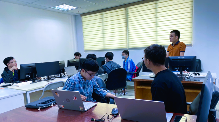
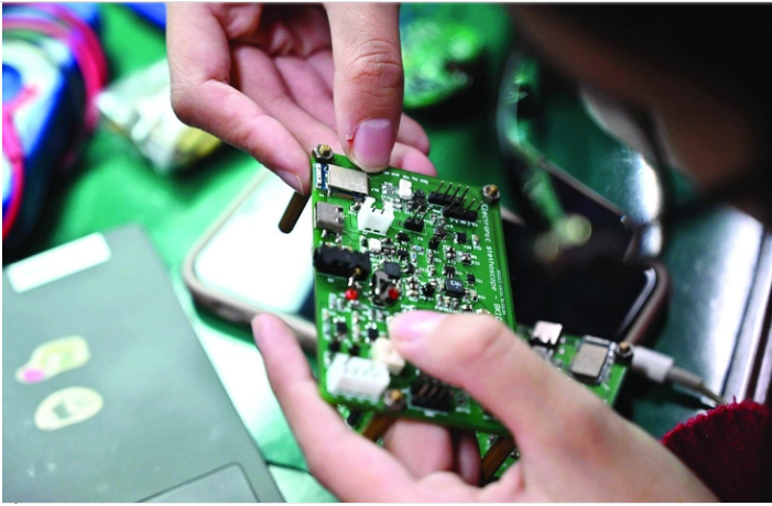
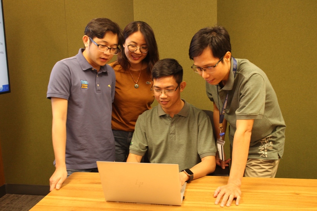
Bạn Có Đam Mê Với Vi Mạch hay Nhúng - Bạn Muốn Trau Dồi Thêm Kĩ Năng
Mong Muốn Có Thêm Cơ Hội Trong Công Việc
Và Trở Thành Một Người Có Giá Trị Hơn
Mong Muốn Có Thêm Cơ Hội Trong Công Việc
Và Trở Thành Một Người Có Giá Trị Hơn
Bạn Chưa Biết Phương Thức Nào Nhanh Chóng Để Đạt Được Chúng
Hãy Để Chúng Tôi Hỗ Trợ Cho Bạn. SEMICON