
Flash Memory has 3 types. They are NAND FLASH, NOR FLASH, SERIAL FLASH.
What is NAND Flash?
NAND is a nonvolatile solid state memory. Nonvolatile memory has the capability to hold and store data even when the power is turned off.
This feature makes NAND an excellent storage solution for many applications such as MP3 players, USB drives, removable storage cards, cell phones, and an endless number of other applications where mobility, power use, speed, and size are key factors.
Functionally, NAND can simply be viewed as a silicon version of a small hard disk drive. NAND is the best memory technology available to provide the necessary cost-per-megabyte and density to become the primary storage device for all systems information, eliminating the need for a separate hard drive in many applications.
How NAND Flash Works
NAND stores data in a large array of transistors. Each transistor can store one bit of data (note that multi-level cell (MLC) NAND can store two bits of data in each cell.) NAND has gained widespread popularity over traditional NOR Flash memory because it can pack a greater number of storage cells in a given area of silicon. This gives NAND Flash density and cost advantages over other nonvolatile memory. NAND achieves these advantages by sharing some of the common areas of the storage transistor, which creates strings of serially connected transistors (in NOR devices, each transistor stands alone). This serial cell architecture explains the device name: NAND (not AND) is the boolean logic reference to how information is read out of these cells.
NAND Flash vs. NOR Flash
In the simplest form, NAND Flash memory is a sequential access device and is best suited to handle data storage like pictures, music, or data files. NOR Flash is designed to be a random access device and is best suited to code storage and execution. Code storage applications include set-top boxes, personal computers, and cell phones. NAND can be used for some boot-up operations, however.
NAND can also be a good high-density replacement for NOR in some instances.
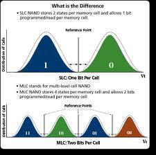
MLC vs. SLC Flash

Traditional, single-level cell (SLC) NAND Flash memory stores one bit of information per memory cell. This basic technology enables faster transfer speeds, lower power consumption, and increased endurance. For designs using mid-range densities, SLC NAND Flash will continue to be a good choice. Multiple-level cell (MLC) NAND, by comparison, stores two to four bits of information per memory cell, effectively doubling the amount of data that can be stored in a similar-size NAND Flash device.
SLC NAND offers high performance and reliability, is supported by all controllers, and requires only 1 bit error correction code (ECC). SLC NAND is for applications like high-performance media cards, hybrid disk drives, solid state drives, and other embedded applications with processors, where it is used for code execution. MLC is a low-cost file storage solution for consumer applications like media players, cell phones, and media cards (USB, SD/MMC, and CF cards) where density is more important than performance. MLC is supported only by controllers that include 4-bit or more ECC.
NAND’s evolution from traditional SLC to low-cost, high-capacity MLC has lowered the cost-per-bit for NAND Flash and opened the way for new applications.
Serial NAND Flash
Serial interfaces are often used for simple, low pin count communication between microcontrollers and system peripherals. Many serial interface configurations exist, but several de facto standards have emerged. One of the best known is the serial peripheral interface (SPI), which has been very popular for applications like code shadowing or storing firmware, BIOS, and similar operating system initialization data. SPI typically uses four pins, including a serial clock, serial data-in, serial data-out, and chip select.
EEPROMs and NOR Flash have dominated SPI memory solutions, but these technologies only offer low-densities options—256Mb at best—that won’t work with the newest designs or an increasing number of new applications. And boosting serial NOR Flash densities to match demand could become cost prohibitive. Enter Serial NAND Flash. Serial NAND Flash has several advantages over earlier SPI memory solutions. First, it’s available in much greater densities, starting at 1Gb, and it offers a lower cost-per-megabit than NOR. On-chip error correction code (ECC) and faster write speeds than NOR are further benefits.
As with all technologies, there are trade-offs. Serial NAND cannot read data as quickly as parallel NAND solutions—a problem serial NOR shares—and designers will have to make software changes to manage NAND’s cache reading and writing features. Finally, Serial NAND is typically available in a VFBGA package and not the NOR-SPI package that many designers are accustomed to. Even with these trade-offs in mind, Serial NAND opens up new possibilities for the SPI interface, and may even be a fit for some applications that currently use a parallel interface but do not require fast read performance.
High-Endurance Enterprise NAND
Enterprise NAND is a high-endurance NAND product family that offers significantly longer cycle endurance than standard NAND.
The ability to store data over a number of WRITE/ERASE cycles is often described as endurance. A typical MLC NAND Flash memory device built on a mature process can endure approximately 5,000 WRITE/ERASE cycles, while a standard SLC NAND Flash device can endure 100,000 cycles or more—which is more than enough for most applications. However, for intensive enterprise applications that require significantly longer cycle endurance, Enterprise NAND is a highly reliable, high-density, high-endurance solution.
Enterprise, or high-endurance, NAND is optimized for high-transaction data processing and high-speed server functions. Offering up to a six-fold and three-fold increase for MLC and SLC NAND, respectively, it far surpasses standard cycle rates and markedly improves product life and performance.
e·MMC Embedded Flash Memory
e·MMC™ embedded memory is a JEDEC-compliant, MultiMediaCard (MMC) device that combines high-quality, low-cost NAND Flash memory with a low-profile BGA package. Because this JEDEC-standard, low-profile package is designed to provide signal compatibility among MMC devices, e·MMC memory provides a high degree of application-to-application interoperability.
With NAND Flash managed by the controller, the necessary software support can be provided by a simple, low-level driver, as shown in the illustration. e·MMC embedded memory essentially transforms a program/erase/read device with bad blocks and bad bits (NAND) into a simple write/read memory. This managed interface addresses potential NAND design concerns internally, using error correction code (ECC), wear leveling, and bad block management technology. Handling errors internally takes the burden off the host controller and increases speed, providing higher system performance. This abstracted solution provides all the necessary NAND Flash functions in an easy-to-use BGA package, saving significant resources that would otherwise go to hardware and software development and speeding time to market.
Jim Cooke, a Micron NAND Flash architect, addresses the various functions that NAND designers face in his white paper Micron® e·MMC™ Embedded Memory Simplifies High-Capacity Storage for Mobile and Embedded Systems.